

As the bandwidth and power demands of AI data centers necessitate a transition from electrical to optical scaleup networking, one component has been conspicuously absent from the co-packaged optics arsenal: the laser itself. That’s no longer the case. Last month, Tower Semiconductor and Scintil Photonics announced production of the world’s first single-chip DWDM light engine for AI infrastructure. DWDM, or dense wavelength division multiplexing, transmits multiple optical signals over a single fiber—greatly reducing power and latency while connecting dozens of GPUs.
Matt Crowley, the CEO of Scintil Photonics, says that the idea of multiplexing optically is not new. Indeed, it’s been around as long as the internet itself. In the 1990s, telecom companies buried huge amounts of optical fiber in the streets, assuming that one wavelength per fiber would eventually become the norm. When the telecom industry realized it possible to transport tens of wavelengths down a single fiber via multiplexing, it revolutionized the industry.
The reason that DWDM has not yet been deployed for data centers specializing in AI applications is that the technology is not yet scalable for cost and needs. “The data transmitted within an AI data center is the equivalent of massively scaling a supercomputer,” Crowley says. In particular, the challenge arises in scale-up networking, or directly connecting accelerators (XPUs, or extended processing units) within a rack or cluster—as opposed to scale-out networking, which connects separate clusters within a data center. Optimizing dozens of GPUs and memory to function as a single entity demands seamless bandwidth and extremely low latency.
To increase bandwidth, reduce latency, and improve energy efficiency in AI data centers, network engineers have gradually been replacing copper links with optical ones. Pluggable transceivers convert electrical signals to optical and vice versa, via discrete optical components integrated onto a single chip: co-packaged optics, or CPO.
“Everything that a big chip company makes involves bonding an optical chip onto their GPU,” says Crowley. The CPO becomes an input/output chip for the processor. But without a scalable way to integrate lasers themselves into the same silicon process flow, it’s been impossible to feed multiple wavelengths per fiber onto one chip. Scintil and Tower will discuss their manufacturing roadmap and details at at the OFC 2026 Conference 17 to 19 March in Los Angeles.
Scintil’s “SHIP” (Scintil Heterogeneous Integrated Photonics) technology integrates lasers, photodiodes, modulators, and other components onto a mass-produced silicon wafer. “It’s our version of CMOS,” says Crowley, but with a few tricks to get around the intrinsic challenges of binding an optical gain material to silicon.
The process starts with a standard 300-millimeter silicon photonics wafer, complete with passive optical components, from Tower Semiconductors. Next, the wafer is flipped upside down to expose its buried oxide layer. Bonding tiny squares of un-patterned InP/III-V semiconductor dies to that layer, precisely where they’re needed at each laser site, minimizes the amount needed of the expensive semiconductor material. Finally, photolithography tools etch diffraction gratings to form eight distributed feedback lasers.
“We’re not re-inventing the laser,” says Crowley. Rather, the advanced photolithography tools translate into more precise spacing and wavelength stability than traditional manufacturing could provide on a silicon wafer.
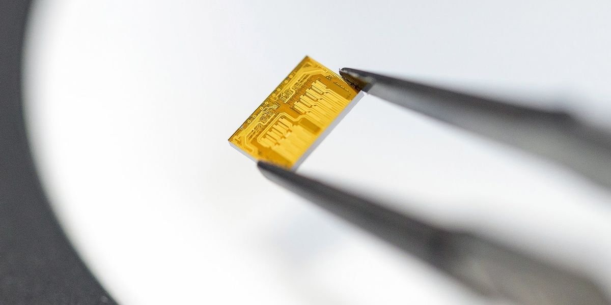
The final product is the “LEAF Light” photonic integrated circuit, a chip that integrates two sets of eight distributed feedback arrays. Each fiber port delivers eight or 16 wavelengths with 100 or 200 gigahertz channel spacing, to ensure no overlap or mode hopping. A second ASIC chip hosts all the electronics to control and monitor the laser array.
Advancing CPO with Multi-Wavelength Lasers
“This is building the laser onto the CPO chip,” says Crowley. Nvidia and Broadcomm have already deployed CPO with a single wavelength per fiber, proving its workability in scale-out networking. “We’re enabling next-generation CPO for scale-up.”
Transmitting multiple wavelengths through a single fiber moves the industry toward a desirable “slow and wide” architecture. For example, instead of transmitting 400 Gb/s over a single channel, or wavelength, the LEAF Light chip spreads 50 Gb/s over 8 channels, greatly increasing the data capacity per fiber and overall power efficiency. The design enables up to 1.6 terabit per second data speeds in a single fiber, and a recent Nvidia roadmap suggested that future DWDM interconnects could eventually enable sub-1 picojoule per bit operations.
Perhaps the most important benefit, according to Crowley, is in latency. “I need to maintain low latency between GPUs,” he says. If any individual processor operates faster than the network overall, the GPUs are always waiting for data bits to process—a problem that’s amplified in scale-up networks with tens or hundreds of GPUs. Forward-processing and error-correction on high-bandwidth channels increases the odds of poor latency. “The utilization rate of the GPUs just tanks,” says Crowley. Using low-bandwidth DWDM to connect multiple GPUs can double utilization.
Scintil and Tower will provide tens of thousands of units to customers by the end of 2026, and plan to increase production by an order of magnitude next year. By 2028, when customers intend to deploy DWDM in scale-up networks, the supply chain will be ready for them. “We’re excited about the possibilities it could open up,” says Crowley.
From Your Site Articles
Related Articles Around the Web

