

This week, over 30,000 people are descending upon San Jose, Calif., to attend Nvidia GTC, the so-called Superbowl of AI—a nickname that may or may not have been coined by Nvidia. At the main event Jensen Huang, Nvidia CEO, took the stage to announce (among other things) a new line of next generation Vera Rubin chips that represent a first for the GPU giant: a chip designed specifically to handle AI inference. The Nvidia Groq 3 language processing unit (LPU) incorporates intellectual property Nvidia licensed from the start-up Groq last Christmas Eve for US $20 billion.
“Finally, AI is able to do productive work, and therefore the inflection point of inference has arrived,” Huang told the crowd. “AI now has to think. In order to think, it has to inference. AI now has to do; in order to do, it has to inference.”
Training and inference tasks have distinct computational requirements. While training can be done on huge amounts of data at the same time and can take weeks, inference must be run on a user’s query when it comes in. Unlike training, inference doesn’t require running costly backpropagation. With inference, the most important thing is low latency—users expect the chatbot to answer quickly, and for thinking or reasoning models inference runs many times before the user even sees an output.
Over the past few years, inference-specific chip start-ups were experiencing a sort of Cambrian explosion, with different companies exploring distinct approaches to speed up the task. The start-ups include D-matrix with digital in-memory compute, Etched with an ASIC for transformer inference, RainAI with neuromorphic chips, EnCharge with analog in-memory compute, Tensordyne with logarithmic math to make AI computations more efficient, FuriosaAI with hardware optimized for tensor operation rather than vector-matrix multiplication, and others.
Late last year, it looked like Nvidia had picked one of the winners among the crop of inference chips, when it announced its deal with Groq. The Nvidia Groq 3 LPU reveal came a mere two and a half months after, highlighting the urgency of the growing inference market.
Memory bandwidth and data flow
Groq’s approach to accelerating inference relies on interleaving processing units with memory units on the chip. Instead of relying on high-bandwidth memory (HBM) situated next to GPUs it leans on SRAM memory integrated within the processor itself. This design greatly simplifies the flow of data through the chip, allowing it to proceed in a streamlined, linear fashion.
“The data actually flows directly through the SRAM,” Mark Heaps said at the Supercomputing conference in 2024. Heaps was a chief technology evangelist at Groq at the time and is now director of developer marketing at Nvidia. “When you look at a multi-core GPU, a lot of the instruction commands need to be sent off the chip, to get into memory and then come back in. We don’t have that. It all passes through in a linear order.”
Using SRAM allows that linear data flow to happen exceptionally fast, leading to the low latency required for inference applications. “The LPU is optimized strictly for that extreme low latency token generation,” says Ian Buck, VP and general manager of hyperscale and high-performance computing at Nvidia.
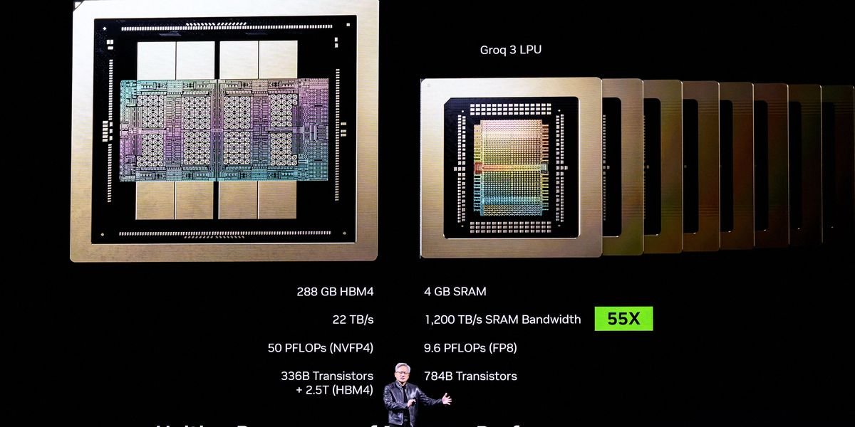
Comparing the Rubin GPU and Groq 3 LPU side by side highlights the difference. The Rubin GPU has access to a whopping 288 gigabytes of HBM and is capable of 50 quadrillion floating-point operations per second (petaFLOPS) of 4-bit computation. The Groq 3 LPU contains a mere 500 megabytes of SRAM memory, and is capable of 1.2 petaFLOPS of 8-bit computation. On the other hand, while the Rubin GPU has a memory bandwidth of 22 terabytes per second, at 150 TB/s the Groq 3 LPU is seven times as fast,. The lean, speed-focused design is what allows the LPU to excel at inference.
The new inference chip underscores the ongoing trend of AI adoption, which shifts the computational load from just building ever bigger models to actually using those models at scale .“NVIDIA’s announcement validates the importance of SRAM-based architectures for large-scale inference, and no one has pushed SRAM density further than d-Matrix,” says d-Matrix CEO Sid Sheth. He’s betting that data center customers will want a variety of processors for inference. “The winning systems will combine different types of silicon and fit easily into existing data centers alongside GPUs.”
Inference-only chips may not be the only solution. Late last week, Amazon Web Services said that it will deploy a new kind of inferencing system in its data centers. The system is a combination of AWS’ Tranium AI accelerator and Cerebras Systems’ third generation computer CS-3, which is built around the largest single chip ever made. The two-part system is meant to take advantage of a technique called inference disaggregation. It separates inference into two parts—processing the prompt, called prefill, and generating the output, called decode. Prefill is inherently parallel, computationally intensive, and doesn’t need much memory bandwidth. While decode is a more serial process that needs a lot of memory bandwidth. Cerebras has maximized the memory bandwidth issue by building more 44 GB of SRAM on its chip connected by a 21 PB/s network.
Nvidia, too, intends to take advantage of inference disaggregation in its new, combined compute tray called the Nvidia Groq 3 LPX. Each tray will house 8 Groq 3 LPUs and a Vera Rubin, which pairs Rubin GPUs with a Vera CPU. The pre-fill and the more computationally intensive parts of the decode are done on Vera Rubin, while the final part is done on the Groq 3 LPU, leveraging the strengths of each chip. “We’re in volume production now,” Huang said.
From Your Site Articles
Related Articles Around the Web

